p-n Junction
Thermal equilibrium condition
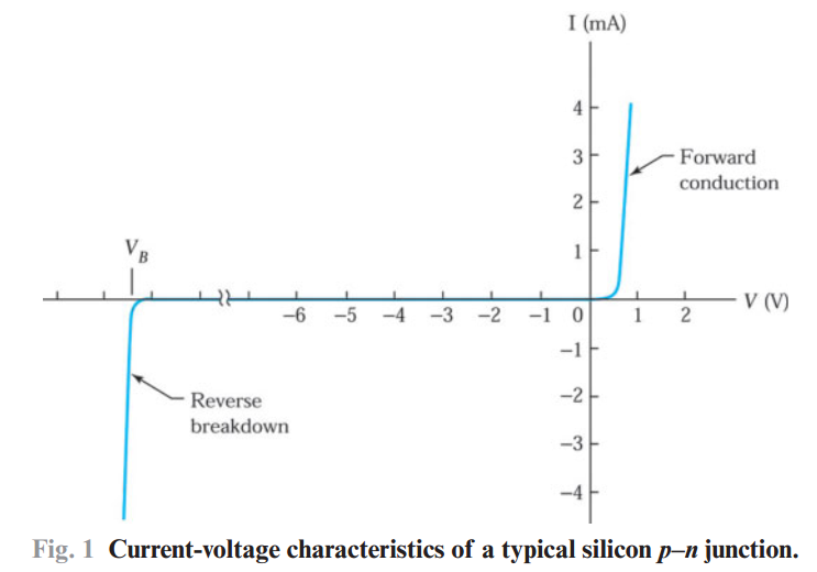
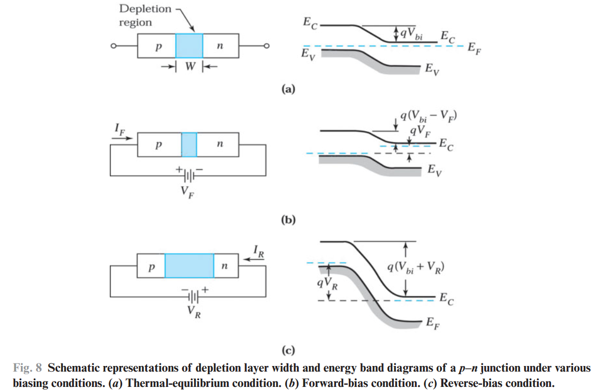
The most important characteristic of p-n junctions is that they recity: they allow current to flow easily in only one direction. The situations of "forward bias" and "reverse bias" are shown below.
(1) For forward bias, the applied voltage is usually less than 1 eV.
(2) For reverse bias, the critical voltage where the current suddenly increase, is called "breakdown voltage", which can vary from just a few volts to many thousands of volts, depending on the doping concentration and other device parameters.
 Band Diagram
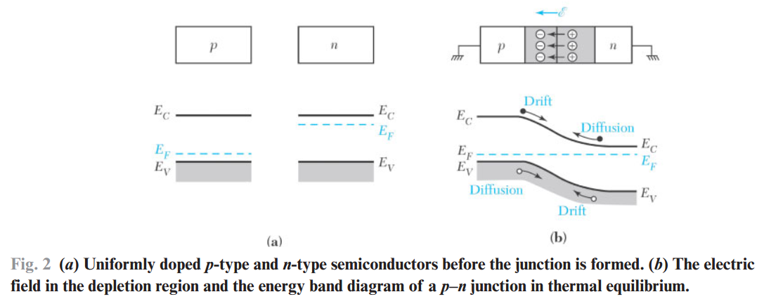 Owing to the diffusion process, for p-type semiconductor, some of the negtive acceptor ions(\(N_{A}^{-} \)) near the junction are left uncompensated because the acceptors are fixed in the semiconductor lattice, whereas the holes are mobile. Simliarly, some of the positive donor ions(\(N_{D}^{+} \)) left uncompensated as the electrons leave the n-side. Consequently, negative space charge forms near the p-side of the junction and a positive space charge forms near the n-side, which finally result in an electric field in the direction opposite to the diffusion current for each type of charge carrier.
Equilibrium Fermi Levels
At thermal equilibrium, i.e. the steady-state condition at a given temperature with no external excitations, the individual electron and hole currents flowing across the junctions are identically zero. Thus, for each type of carrier the drift current due to the electric field must exactly cancel the diffusion current due to the concentration gradient. $$\begin{aligned} J_{p} &=J_{p}(\text { drift })+J_{p}(\text { diffusion }) \\ &=q \mu_{p} p E-q D_{p} \displaystyle\frac{d p}{d x} \\ &=q \mu_{p} p\left(\displaystyle\frac{1}{q} \frac{d E_{i}}{d x}\right)-k T \mu_{p} \displaystyle\frac{d p}{d x}=0 \end{aligned}$$Note that \( E \) means electric field, while \(E_i \) means electrostatic potential. Also, recall \( -q E=-(\text { gradient of electron potential energy })=-\displaystyle\frac{d E_{C}}{d x}\) and Einstein relation \( D_{p}=(k T / q) \mu_{p} \). Then substituting the expression for hole concentration $$ p=n_{i} e^{\left(E_{i}-E_{F}\right) / k T}$$ and its derivative $$\frac{d p}{d x}=\frac{p}{k T}\left(\frac{d E_{i}}{d x}-\frac{d E_{F}}{d x}\right)$$ into the \( J_{p}\) expression and yields the net hole current density $$J_{p} = \mu_{p} p \frac{d E_{F}}{d x} = 0$$ or $$\frac{d E_{F}}{d x}=0$$ Similar situation occur for net electron current density. Thus, for the condition of zero net electron and hole currents, the Fermi level must be constant (i.e., independent of \( x \)) throughout the sample.
The constant Fermi level required at thermal equilibrium results in a unique space charge distribution at the junction. The unique space charge distribution and the electrostatic potential \(\psi\) are given by Poisson’s equation: $$\frac{d^{2} \psi}{d x^{2}} \equiv \frac{d \mathscr{E}}{d x} =\frac{\rho_{s}}{\varepsilon_{s}}= \frac{q}{\varepsilon_{s}}\left(N_{D}^+- N_{A}^-+p - n\right)$$ Here we assume that all donors and acceptors are ionized.
In the region far away from the metallurgical junction, charge neutrality is maintained and the total space charge density is zero. $$\frac{d^{2} \psi}{d x^{2}}= 0 \quad\quad\quad N_{D}^+-N_{A}^-+p-n=0$$For a p-type neutral region, we assume \(N_{D}^+=0 \) and \(p>>n \). By setting \(N_{D}^+=n=0 \) , plus \( p=N_{A}^- \)(neutrality requirement), we obtain the electrostatic potential of the p-type neutral region with respect to the Fermi level:$$\psi_{p} \equiv-\left.\frac{1}{q}\left(E_{i}-E_{F}\right)\right|_{x \leq x_{p}}=-\frac{k T}{q} \ln \left(\frac{N_{A}}{n_{i}}\right)$$ Note that \( E_{i}-E_{F} \) is obtained from \(p=n_{i} e^{\left(E_{i}-E_{F}\right) / k T}\).
For n-type neutral region, we obtain $$\psi_{n} \equiv-\left.\frac{1}{q}\left(E_{i}-E_{F}\right)\right|_{x \geq x_{n}}=\frac{k T}{q} \ln \left(\frac{N_{D}}{n_{i}}\right)$$ The total electrostatic potential difference between the p-side and the n-side neutral regions at thermal equilibrium is called the built-in potential \(V_{b i} \)$$V_{\mathrm{bi}}=\psi_{\mathrm{n}}-\psi_{\mathrm{p}}=\frac{k T}{q} \ln \left(\frac{N_{\mathrm{A}} N_{\mathrm{D}}}{n_{\mathrm{i}}{ }^{2}}\right)$$
Note that p-n junction has the same host semiconductor in two sides. Therefore, the difference between \(E_C\) in two sides is the as the difference between \(E_i\) in two sides.
Space Charges
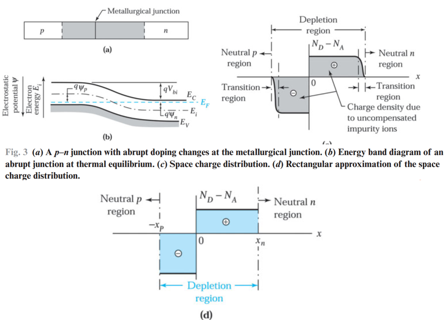 Narrow transition region: the space charge of impurity ions is partially compensated by the mobile carriers. For Si and GaAs p-n junctions, width of each transition region is small compared with the width of the depletion region. Therefore, we can neglect this region.
Completely depleted region: mobile carrier densities are zero, this region is called the depletion region (also the space-charge region). For this region, we have (Poisson’s equation):(for the completely depleted region, \(p=n=0\)) $$\frac{d^{2} \psi}{d x^{2}}= \frac{q}{\varepsilon_{s}}(N_{A}^- - N_{D}^+)$$
Depletion region
To solve Poisson’s equation we must know the impurity distribution. Here we consider two important cases:
(1) Abrupt junction: a p–n junction formed by shallow diffusion or low-energy ion implantation.
(2) Linearly graded junction: formed by deep diffusions or high-energy ion implantations.
Abrupt junction
In the depletion region, free carriers are totally depleted so that Poisson’s equation simplifies to $$\begin{array}{l} \displaystyle\frac{\mathrm{d}^{2} \psi}{\mathrm{d} x^{2}}=\frac{q N_{\mathrm{A}}}{\varepsilon_{\mathrm{s}}}, \quad-x_{\mathrm{p}} \leqslant x<0 ; \\ \displaystyle\frac{\mathrm{d}^{2} \psi}{\mathrm{d} x^{2}}=-\frac{q N_{\mathrm{D}}}{\varepsilon_{\mathrm{s}}}, \quad 0<x \leqslant x_{\mathrm{n}} . \end{array}$$The overall space charge neutrality requires \( N_{A} x_{p}=N_{D} x_{n} \), and the total depletion layer width \(W\) is given by \(W= x_{p}+x_{n}\).
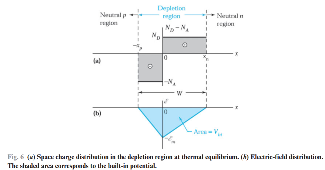 The electric field shown is obtained by integration, which gives(note minus sign) $$\begin{array}{l} E(x)=-\displaystyle\frac{\mathrm{d} \psi}{\mathrm{d} x}=-\frac{q N_{\mathrm{A}}\left(x+x_{\mathrm{p}}\right)}{\varepsilon_{\mathrm{s}}}, \quad-x_{\mathrm{p}} \leqslant x<0 \\ E(x)=-E_{\mathrm{m}}+\displaystyle\frac{q N_{\mathrm{D}} x}{\varepsilon_{\mathrm{s}}}=\frac{q N_{\mathrm{D}}}{\varepsilon_{\mathrm{s}}}\left(x-x_{n}\right), \quad 0<x \leqslant x_{\mathrm{n}}\end{array}$$ At \(x = 0\), we have $$E_{\mathrm{m}}=\frac{q N_{\mathrm{D}} x_{\mathrm{n}}}{\varepsilon_{\mathrm{s}}}=\frac{q N_{\mathrm{A}} x_{\mathrm{p}}}{\varepsilon_{\mathrm{s}}}=\frac{q N_{\mathrm{B}} W}{\varepsilon_{\mathrm{s}}}$$where \( N_{\mathrm{B}}=\frac{N_{\mathrm{A}} N_{\mathrm{D}}}{N_{\mathrm{A}}+N_{D}}\)
The built-in potential( triangle area): $$\begin{aligned} V_{b i} &=-\int_{x_{p}}^{x_{n}} E(x) d x=-\left.\int_{x_{p}}^{0} E(x) d x\right|_{p \text { side }}-\left.\int_{0}^{x_{n}} E(x) d x\right|_{n \text { side }} \\ &=\frac{q N_{A} x_{p}^{2}}{2 \varepsilon_{s}}+\frac{q N_{D} x_{n}^{2}}{2 \varepsilon_{s}}=\frac{1}{2} E_{m} W \end{aligned}$$With \(N_{A} x_{p}=N_{D} x_{n}\), we obtain the total depletion layer width as a function of the built-in potential $$W=\sqrt{\frac{2 \varepsilon_{s}}{q}\left(\frac{N_{A}+N_{D}}{N_{A} N_{D}}\right) V_{b i}}$$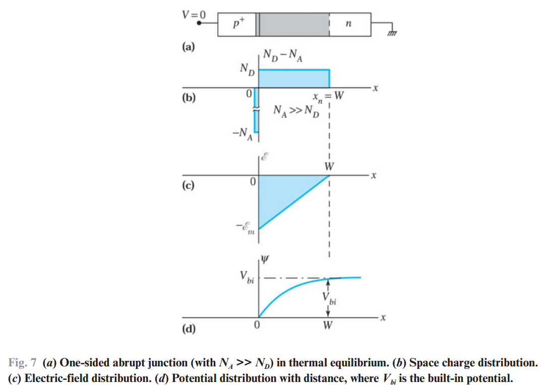 When the impurity concentration on one side of an abrupt junction is much higher than that on the other side, the junction is called a one-sided abrupt junction. The expression for \( W \) can be simplified to$$W \cong x_{n}=\sqrt{\frac{2 \varepsilon_{s} V_{b i}}{q N_{D}}}$$
For the above figures(not one-side abrupt junction any more), the depletion layer widths are: $$W=\sqrt{\frac{2 \varepsilon_{\mathrm{s}}\left(V_{\mathrm{bi}}\pm V\right)}{q N_{\mathrm{B}}}}$$where minus/plus depends on forward-bias/reverse-bais condition.
Linearly graded junction
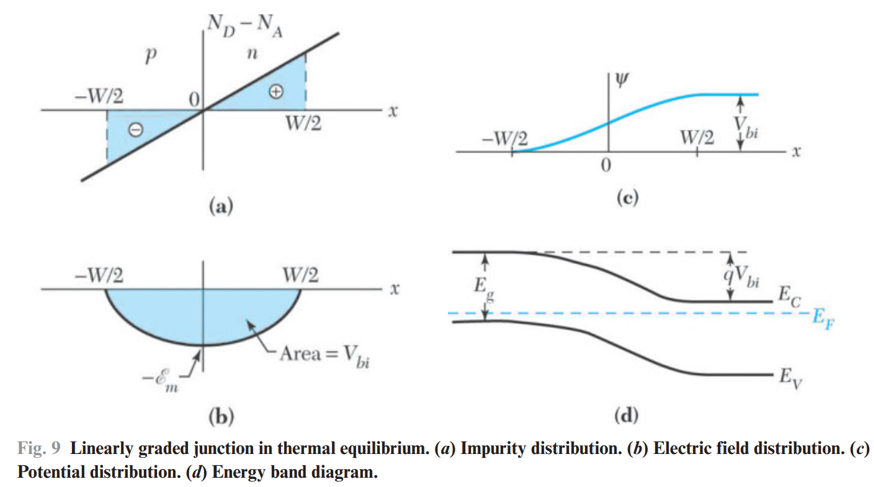
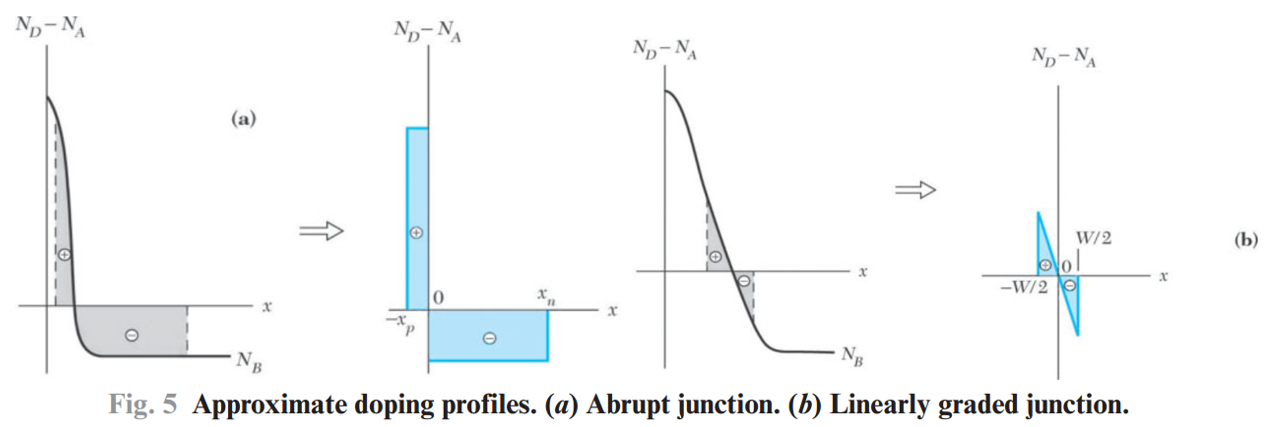
We first consider the case of thermal equilibrium. The impurity distribution for a linearly graded junction is shown below. The Poisson’s equation for the case is $$\frac{\mathrm{d}^{2} \psi}{\mathrm{d} x^{2}}=-\frac{\mathrm{d} E}{\mathrm{~d} x}=-\frac{\rho_{\mathrm{s}}}{\varepsilon_{\mathrm{s}}}=-\frac{q}{\varepsilon_{\mathrm{s}}} a x, \quad-\frac{W}{2} \leqslant x \leqslant \frac{W}{2}$$where \( \alpha \) is the impurity gradient. The electric-field distribution is $$\mathscr{E}(x)=-\frac{q a}{\varepsilon_{s}}\left[\frac{(W / 2)^{2}-x^{2}}{2}\right]$$ The maximum field at \(x = 0\) is $$\mathscr{E}_{m}=\frac{q a W^{2}}{8 \varepsilon_{s}}$$. The built-in potential and the depletion layer width are given by $$\begin{array}{l}V_{\mathrm{bi}}=\displaystyle\frac{q a W^{3}}{12 \varepsilon_{\mathrm{s}}} \\ W=\left(\displaystyle\frac{12 \varepsilon_{\mathrm{s}} V_{\mathrm{bi}}}{q a}\right)^{1 / 3}\end{array}$$
Depletion capacitance
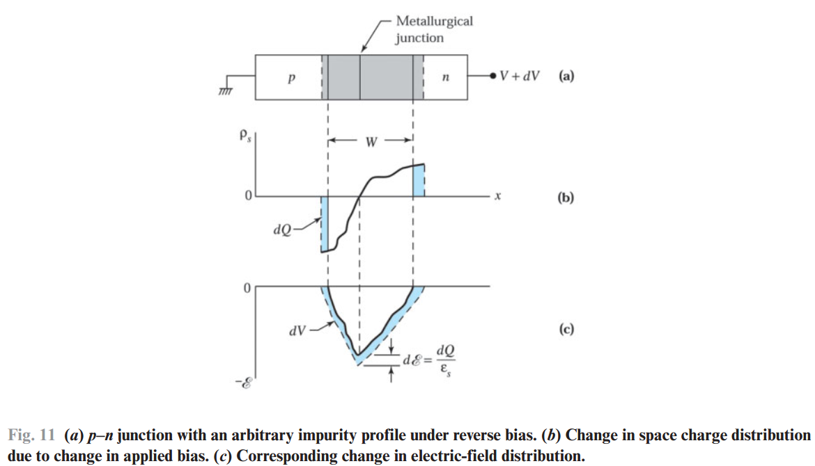
The junction depletion-layer capacitance per unit area is defined as \(C_{j}=d Q / d V\), where \(d Q \) is the incremental change in depletion-layer charge per unit area for an incremental change in the applied voltage \(d V\).
Note that we are talking about capacitance per unit area, not the normal capacitance, and the dimension difference is the quare of the length. Therefore, \( \mathrm{d} E=\mathrm{d} Q / \varepsilon \) is valid when compared with the normal case of point charge \(E=\displaystyle\frac{Q}{4 \pi \varepsilon_{0} r^{2}}\)
Solid lines --- a voltage \(V\) applied to the n-side.
Dashed lines --- a voltage \(V+dV\) applied to the n-side.
Poisson’s equation --- \(\mathrm{d} E=\mathrm{d} Q / \varepsilon\).
Colored area --- incremental change in the applied voltage \(d V\).$$C_{j} \equiv \frac{\mathrm{d} Q}{\mathrm{~d} V}=\frac{\mathrm{d} Q}{W \frac{\mathrm{d} Q}{\varepsilon_{\mathrm{s}}}}=\frac{\varepsilon_{\mathrm{s}}}{W}$$or $$C_{j}=\frac{\varepsilon_{s}}{W}$$with a unit \(\mathrm{F} / \mathrm{cm}^{2}\).
For a one-sided abrupt junction, we obtain $$C_{\mathrm{j}}=\frac{\varepsilon_{\mathrm{s}}}{W}=\sqrt{\frac{q \varepsilon_{\mathrm{s}} N_{\mathrm{B}}}{2\left(V_{\mathrm{bi}}-V\right)}}$$Note that the above disscusion is for the reverse-bais condition in which we can assume that only the variation of the space charge in the depletion region contributes to the capacitance. However, this is not valid for forwards-bais condition when considering a large number of mobile carriers across the junction.
The incremental change of these mobile carriers with respect to the biasing voltage contributes an additional term, called the diffusion capacitance, which will be discussion in another chapter.
Current-voltage characteristics
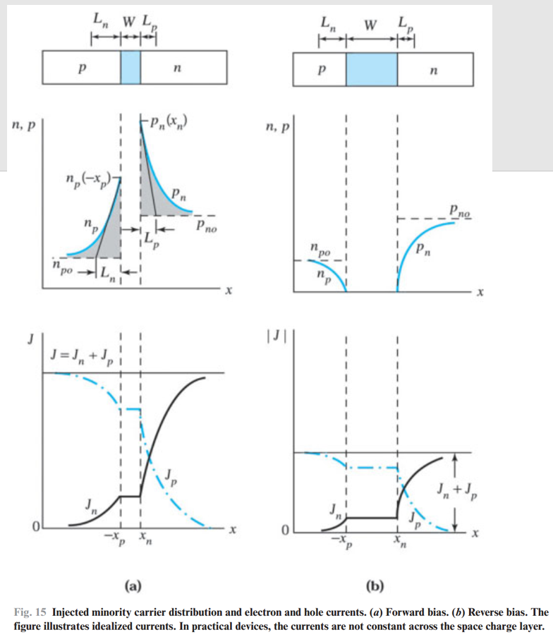
Under forward-bias, minority carrier injections occur, that is, electrons are injected into the p-side, whereas holes are injected into the n-side.
Ideal Characteristics
Ideal current-voltage characteristics based on the following assumptions:
(1) the depletion region has abrupt boundaries and, outside the boundaries, the semiconductor is assumed to be neutral;
(2) the carrier densities at the boundaries are related by the electrostatic potential difference across the junction;
(3) the low-injection condition, that is, the injected minority carrier densities are small compared with the majority carrier densities (in other words, the majority carrier densities are changed negligibly at the boundaries of neutral regions by the applied bias);
(4) neither generation nor recombination current exists in the depletion region and the electron and hole currents are constant throughout the depletion region.
current density equations and continuity equations, describing the motion of the carriers $$\begin{aligned} &J_{n}=q \mu_{n} n \varepsilon+q D_{n} \frac{\partial n}{\partial x} \\ &J_{p}=q \mu_{p} p \varepsilon-q D_{p} \frac{\partial p}{\partial x} \\ &\frac{\partial n_{p}}{\partial \tau}=\frac{1}{q} \frac{\partial J_{n}}{\partial x}-\frac{\Delta n_{p}}{\tau_{n}} \\ &\frac{\partial p_{n}}{\partial \tau}=-\frac{1}{q} \frac{\partial J_{p}}{\partial x}-\frac{\Delta p_{n}}{\tau_{p}} \end{aligned}$$
Clear picture here.
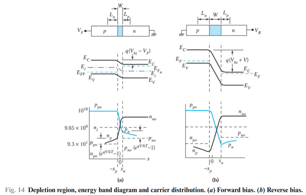
From the section of thermal equilibrium, we know \(V_{\mathrm{bi}}=\displaystyle\frac{k T}{q} \ln \left(\frac{N_{\mathrm{A}} N_{\mathrm{D}}}{n_{\mathrm{i}}^{2}}\right)\) (At thermal equilibrium, the majority carrier density in the neutral regions is essentially equal to the doping concentration). Therefore, here we have $$V_{b i}= \frac{k T}{q} \ln \frac{p_{p o} n_{n o}}{n_{i}^{2}} = \frac{k T}{q} \ln \frac{n_{n o}}{n_{p o}}$$Rearrange this equation gives $$n_{n o} = n_{p o} \text{exp}({q V_{b i} / k T})$$When a bias is applied, we have$$n_{n} = n_{p} \text{exp}({q(V_{b i}-V) / k T})$$with \(V\) positive for forward bias and negative for reverse bias. For the low-injection condition, the approximation \(n_{n} \cong n_{n o} \) holds true. Therefore \(n_{p o} \exp \left(q V_{b i} / k T\right)=n_{p} \exp \left(q\left(V_{b i}-V\right) / k T\right) \), which can be simplified to $$n_{p}= n_{p o} \text{exp}(e^{q V / k T})$$ or $$n_{p}-n_{po}= n_{p o} (\exp (q V / k T)-1)$$Similarily, we have $$p_n- p_{no}= p_{no}(\text{exp}(q V / k T)-1)$$Under our idealized assumptions, no current is generated within the depletion region; all currents come from the neutral regions. In the neutral n-region, there is no electric field, thus the steady-state continuity equation reduces to$$\frac{d^{2} p_{n}}{d x^{2}} -\frac{p_{n} -p_{\text {no }}}{D_{p} \tau_{p}}=0$$With the boundary condition \(p_{n}-p_{n o}=p_{n o}(\exp (q V / k T)-1)\) and \( p_{n}(x=\infty)=p_{n o}\), the solution gives$$p_{\mathrm{n}}-p_{\mathrm{n} 0}=p_{\mathrm{n} 0}\left[\exp \left(\frac{q V}{k T}\right)-1\right] \exp \left[\frac{-\left(x-x_{\mathrm{n}}\right)}{L_{\mathrm{p}}}\right]$$where \(L_p =\sqrt{D_{p} \tau_{p}}\) is the diffusion length of holes (minority carriers) in the n-region. Because the current is constant throughout the device, we just look at the current at \( x=x_{\mathrm{n}} \), then we get $$J_{\mathrm{p}}\left(x_{\mathrm{n}}\right)=-\left.q D_{\mathrm{p}} \frac{\mathrm{d} p_{\mathrm{n}}}{\mathrm{d} x}\right|_{x_{n}}=\frac{q D_{\mathrm{p}} p_{\mathrm{n} 0}}{L_{\mathrm{p}}}\left[\exp \left(\frac{q V}{k T}\right)-1\right]$$ Similarly, we obtain for the neutral p-region, the diffusion electron density is $$J_{\mathrm{n}}\left(-x_{\mathrm{p}}\right)=\frac{q D_{\mathrm{n}} n_{\mathrm{p} 0}}{L_{\mathrm{n}}}\left[\exp \left(\frac{q V}{k T}\right)-1\right]$$ The total current density is ( the ideal diode equation, or Shockley diode equation) $$\begin{array}{c} J=J_{\mathrm{p}}\left(x_{\mathrm{n}}\right)+J_{\mathrm{n}}\left(-x_{\mathrm{p}}\right)=J_s\left[\exp \left(\displaystyle\frac{q V}{k T}\right)-1\right] \\ J_{\mathrm{s}} \equiv \displaystyle\frac{q D_{\mathrm{p}} p_{\mathrm{n} 0}}{L_{\mathrm{p}}}+\displaystyle\frac{q D_{\mathrm{n}} n_{p 0}}{L_{\mathrm{n}}} \end{array}$$ where \(J_{s}\) is the saturation current density.
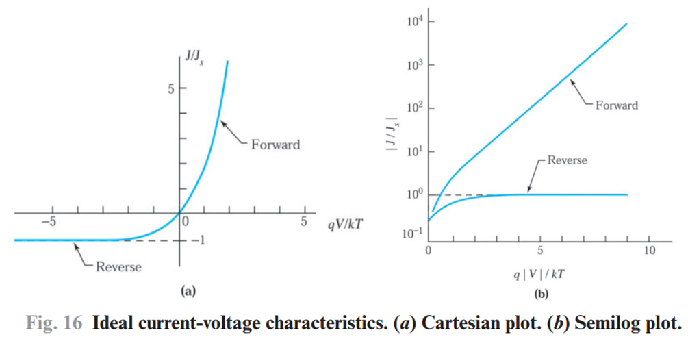
(1) In the forward direction with positive bias on the p-side, for \(V \geq 3 k T l q\), the rate of current increase is constant
(2) At \(300 \, \mathrm{K} \) for every decade change of current, the voltage change for an ideal diode is \(60 \mathrm{mV}(=2.3 kT / q)\). In the reverse direction, the current density saturates at \( -J_s \)
The total current for \(p^{+}-n\) junction(one-side abrupt junction) is $$J=\frac{q D_{p} p_{n o}}{L_{p}}(\text{exp}({q V / k T})-1)=\frac{q D_{p}}{L_{p}} N_{V}(\text{exp}({[q V-(E_{F}-E_{V})] / k T})-1)$$
Chagre storage and transient behavior
Junction breakdown
Heterojunction
好的资料/重要人物
埃德蒙·贝克勒尔:人们很早就盯上了太阳能,并尝试将其转化成可直接使用的电能。最笨的方法就是用太阳光提供热来烧开水,然后用开水的蒸汽来发电。但是每次能量的转化必然伴随着消耗,烧开水方法的效率不高。因此人们陷入了沉思:怎样把太阳能直接变成电能呢?1839年的某一天,研究磷光的埃德蒙发现了不得了的东西,他把氯化银放在酸溶液里,再接两个铂电极,然后拿到太阳下去晒,结果在两个电极中间发现了电压! 当时人们还不知道该现象的原理,只知道光照可以产生电势,于是把这种现象叫做光生伏特效应,简称光伏效应。现在的太阳能电池基本都是利用了光伏效应,所以太阳能电池也叫太阳能光伏电池。
他也知名于萤光和磷光方面研究的贡献,也是发现天然放射性的亨利·贝克勒之父。
科普