图床 Materals-img/
Materials Science-Teaching & Learning Packages-剑桥大学
材料介绍-威斯康辛大学 各种演示-威斯康辛大学
Microstructural Evolution in Materials-MIT 对应的EDX
Solid State Chemistry-Aalto大学
材料中的缺陷
- A perfect crystal could exist only at absolute zero. At all finite temperatures, crystals are imperfect
– Atoms vibrate, which may be regarded as a form of defect
– Some atoms are always misplaced - In some crystals, the number of defects may be very small (<<1%) as in, e.g., highpurity silicon, diamond, or quartz.
- In highly defective crystals, the defects may in fact be regarded as a fundamental part of the structure rather than an imperfection.
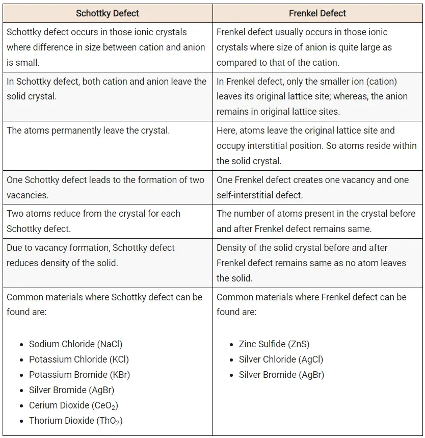
弗伦克尔缺陷

指晶体结构中由于原先占据一个格点的原子(或离子)离开格点位置,成为间隙原子(或离子),并在其原先占据的格点处留下一个空位,这样的空位-间隙对就称为弗仑克尔缺陷。
- An atom displaced off its lattice site into an interstitial site that is normally empty
- AgCl (with the NaCl crystal structure) has predominantly this defect (interstitial Ag)
- There is probably some covalent interaction between the interstitial Ag+ ion and its four Cl− neighbours which stabilizes the defect
– Due to this, AgCl prefers Frenkel defects over Schottky defects - Comparison with NaCl: Na+ is a “harder” cation and there would be high energetic cost to have it surrounded by four other Na+ ions
– Frenkel defects do not occur to any significant extent in NaCl - Calcium fluoride, CaF2, has predominantly anion Frenkel defects in which F− occupies interstitial sites
- As with Schottky defects, the vacancy and interstitial are oppositely charged and may attract each other to form a pair.
肖特基缺陷
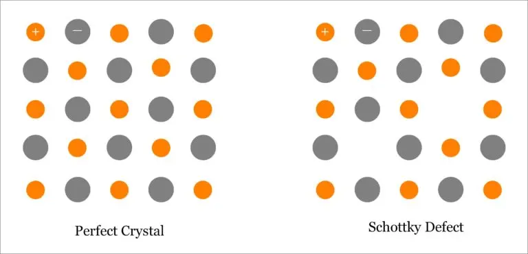
肖特基缺陷是由于晶体表面附近的原子热运动到表面,在原来的原子位置留出空位,然后内部邻近的原子再进入这个空位,这样逐步进行而造成的,看来就好像是晶体内部原子跑到晶体表面来了。重要特点是,阴阳离子空位成对出现。
- Schottky defect is a typical stoichiometric defect in ionic solids such as halides or oxides
– Pair of vacant sites: an anion vacancy and a cation vacancy
– Principal point defect in alkali halides - To compensate for the vacancies, there should be two extra atoms at the surface of the crystal for each Schottky defect
- Equal numbers of anion and cation vacancies required to preserve local electroneutrality
- Vacancies attract each other and tend to associate (ΔHassociation ≈ 120 kJ/mol)
- For NaCl at room temperature, typically one in 1015 of the sites is vacant
- In other terms, 1 mg of NaCl (~1019 atoms) contains ~104 Schottky defects
- Schottky defects are responsible for the optical and electrical properties of NaCl
无外场作用时,热缺陷在晶体内部作无规则布朗运动;当存在外场(可以是力 场、电场、浓度场等)时,热缺陷可以作定向运动。正因为如此,才使晶体中的各种传输过程(离 子导电、传质等)及高温动力学过程(扩散、烧结等)能够进行。
色心
概述
Term: A crystal defect that absorbs light in a spectral region in which the crystal itself does not absorb light.
(1) 狭义概念
Originally, the term "color centers" was applied only to F-centers (德国人发现的碱金属卤化物中卤离子空位trapped an electron).
(2) 广义概念
This term later came to include all point lattice defects that absorb light in a region where the crystal itself does not absorb. Such defects may constitute intrinsic centers or impurity centers. The former encompass positive-ion vacancies, negative-ion vacancies, and interstitial ions; the latter, impurity atoms and ions. Color centers are found in many inorganic crystals and in glasses. They are very common in naturally occurring minerals.
Intrinsic centers(两类): may be produced by photochemcial coloration, that is, by exposing a crystal to ionizing radiation or to light corresponding to the region where the crystal iteself absorbs light. Such color centers are said to be induced. In photochemical coloration, nonequilibrium charge carriers (conduction electrons and holes), which are generated upon exposure to radiation, are trapped by crystal defects and change their charge, resulting in the appearance of new bands in the absorption spectrum and a change in the color of the crystal. At least two types of color centers are usually distinguished, namely, those with trapped electrons and those with trapped holes. If the particles or photons that produce the coloration have sufficiently high energy, they may produce new defects (see RADIATION-INDUCED DEFECTS IN CRYSTALS). The new defects also usually occur in pairs, for example, a vacancy and an interstitial ion.
Bleaching of Intrinsic centers(可能发光): Induced color centers may be destroyed by thermal bleaching —that is, by heating—or by bleaching with light—that is, by exposure to light corresponding to the spectral region in which the centers absorb light. Upon exposure to heat or light, a charge carrier—for example, an electron—is liberated from the defect that trapped it and recombines with a hole. This process may be accompanied by luminescence if the energy released is emitted as a photon. Defect pairs may also disappear upon exposure to heat; for example, an interstitial atom may occupy the corresponding vacancy. In this case, luminescence, as a rule, is not observed because all the energy released is converted into heat.
Additive coloration(更稳定): In another method of producing intrinsic centers, called additive coloration, the charge carriers that are necessary for the formation of color centers are introduced into the crystal rather than being generated in it. Hence, the process is called additive coloration, that is, coloration by the addition of something. Additive coloration is achieved by
(1) heating a crystal in a metal vapor
(2) introducing electrons into a heated crystal from a point cathode
(3) means of electrolysis.
When a crystal is heated in a metal vapor, the metal atoms diffuse into the crystal, occupy positive-ion vacancies, and form F-centers by donating electrons to negative-ion vacancies. In some cases, such as fluorite, intrinsic centers may be produced during crystallization. Color centers formed by additive coloration cannot be destroyed by heat or light alone. Thus, additively colored alkali halide crystals are bleached by heating in a halogen atmosphere, and colorless fluorite may be obtained by altering the crystallization conditions.
注:Additive coloration results in the formation of only electron centers, while radiation coloring leads to the formation of electron and hole centers. 来自文献。
参考资料:
(1) 色心晶体-百度文库
(2) color center-苏联大百科全书
(3) F-Centers-威斯康辛麦迪逊大学
(4) The Imperfect SolidColor Centers in Ionic Crystals
(5) Color Centers-RP-photonics
(6) Introduction to solid state physics-Kittel-Chapter20
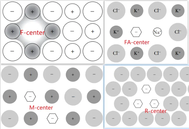
\(F\)心及其变体
色心是德国哥廷根大学的波尔发现的,他将碱金属卤化物晶体在金属蒸汽中加热然后骤冷,得到的各种各样颜色的晶体,他将其归因于晶格缺陷造成的光吸收。我们经常举的例子就是NaCl晶体在Na蒸汽中加热,然后快速冷却到室温,可以得到黄色的晶体。吸收对应的色心就是\(F \)心,其实质就是一个负离子空位和被它俘获的电子。如果这个色心俘获一个电子还不满足,再俘获一个就会形成\(F^{-}\)。如果\(F \)心的电子跑了,就形成\(F^{+}\)。
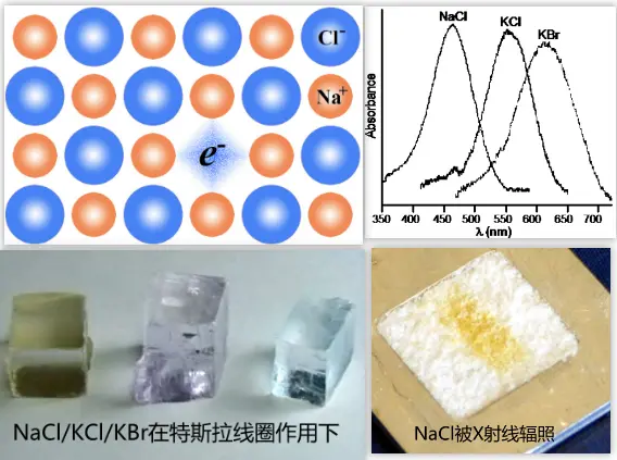 上图中的NaCl被辐照后颜色能稳定存在;但是KBr辐照后的不稳定,the KBr sample decayed so fast that it had to be viewed inside the cabinet of the diffractometer。F-Centers-威斯康辛麦迪逊大学
F-center absorption band: F-centers have been studied in the greatest detail in alkali halide crystals. However, they have also been observed in other crystals. An F-center in an alkali halide crystal gives rise to a selective bell-shaped absorption band called an F-band. The F-band usually lies in the visible region of the spectrum. For crystals with the same negative ions but different positive ions or with different negative ions but the same positive ions, the F-band is shifted to longer wavelengths as the atomic weight of the positive ions (in the former case) or of the negative ions (in the latter case) increases. For example, the F-band in NaCl has an absorption peak in the blue region (λ = 465 nm), and the color of the crystal is yellow-brown (the complementary color). The F-band in KCl has an absorption peak in the green region (λ = 563 nm), and the crystal appears violet.
The trapped electron provides a classic example of an “electron in a box”
– A series of energy levels are available for the electron within this “box”
– The energy required to transfer the electron from one level to another falls in the visible part of the electromagnetic spectrum.
Complex F-center: Other, more complex intrinsic centers have also been observed in alkali halide crystals. Such color centers include F2- (or M-) centers, F3- (or R-) centers, and F4- (or N-) centers, which are, respectively, two, three, and four bound F-centers (that is, two, three, or four negative-ion vacancies that have trapped two, three, or four electrons). F2+-centers and F3+-centers also exist; they are, respectively, ionized F2-centers and ionized F3-centers.
Other defect centers identified in the alkali halides include 参考
– F'-center: two electrons trapped on an anion vacancy
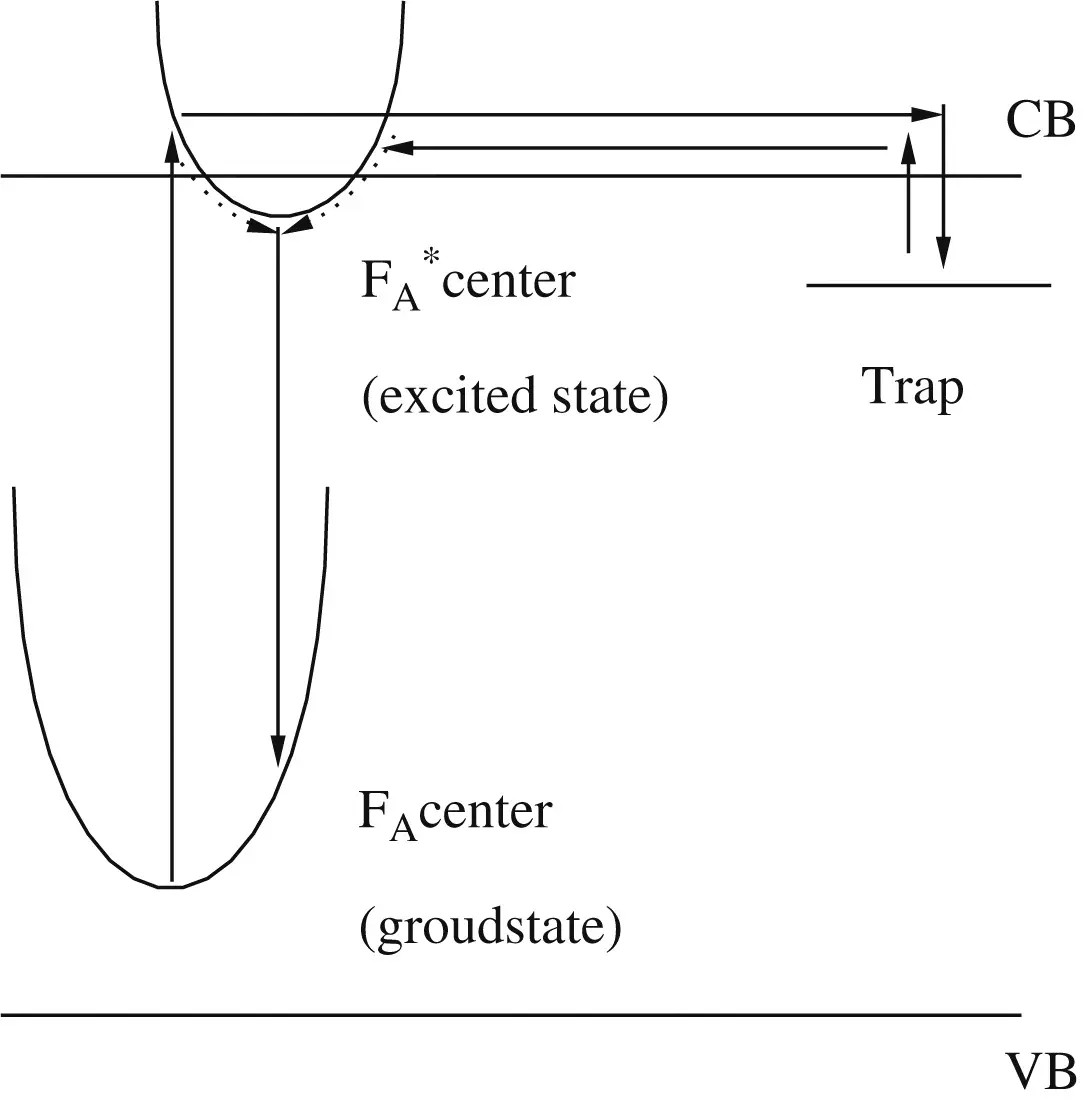
– FA-center: an F-center, consists of an F center with one neighbouring positive ion replaced by a positive ion of a different kind.
实例:Na+ in KCl, one of six cationic neighbors is a foreign monovalent cation.
两种类型:FA(I) and FA(II) depending on the type of replacement ion. FA(I) centers have similar properties as regular F centers, whereas FA(II) centers cause two potential wells to form in the excited state due to the repositioning of a halide ion.
FA center is known as a potential luminescence center.[JL-2009]
– FB-center: consists of an F center with two neighbouring positive ions replaced by a positive ion of a different kind. The FB centers are also divided into two groups, FB(I) and FB(II), with similar behaviour to the FA(I) and FA(II) centers. Due to the statistical nature of the distribution of impurity ions, FB centers are much more rare than FA centers.
– M-center: a pair of nearest neighbor F-centers
– R-center: three nearest neighbor F-centers located on a (111) plane
– Z-centers: in alkali halides are F-centers associated with vacancies and divalent impurity ions, such as Ca or Sr.
– Ionized or charged cluster centers, such as M+, R+ and R−
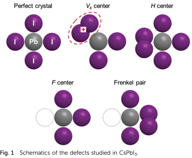
\(V_K\)心和H心
(1) \(V_K\)心
这里就讲一下其中的自陷(self-trapped)空穴型色心,也就是\(V_K\)心。比如在KCl晶体中,两个沿着(110)相邻的卤素例子X-共有一个自陷空穴,构成一个卤素分子离子X2-, 称为\(V_K\)心。
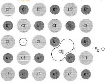
The antimorph to the F center is a hole trapped at a positive ion vacancy, but no such center has been identified experimentally in alkali halides; in insulating oxides the O- (called V-) defect is known. The best-known trappedhole center is the VK center, 上图. The VK center is formed when a hole is trapped by a halogen ion in an alkali halide crystal. Electron spin resonance shows that the center is like a negative halogen molecular ion, such as Cl2- in KCl. The Jahn-Teller trapping of free holes is the most effective form of selftrapping of charge carriers in perfect crystals.
参考Introduction to solid state physics-Kittel-Chapter20
有的时候容易将\(F \)心和\(V_K\)心记混了,我们可以这样想,高能射线或者UV打到样品上,于是形成了空穴-电子对,空穴在价带上,电子在导带上,然后空穴被缺陷俘获,即形成了\(V_K\)心,电子被缺陷俘获形成\(F \)心。
(2) H-心(center)
Color centers with trapped holes in alkali halide crystals are molecular ions of a halogen (for example, Cl) that have trapped a hole (that is, donated an electron) and that either occupy the position of two normal ions, forming a VK-center, or occupy the position of a single normal ion, forming an H-center. Both are stable at low temperature only.(这句是对的吗?) (固体发光材料—P86讲了这部分)
Impurity centers
Impurity centers are foreign atoms or ions that are introduced into a crystal, glass, or some other host material. To produce impurity centers in crystals, the impurity is added to the melt or solution during crystallization or is diffused into a prepared crystal. As is the case with other point defects, impurity atoms and ions may trap electrons or holes, resulting in a change in the absorption band or the color of the crystal. In crystals and glasses that contain impurities, induced impurity centers are produced during photochemical coloration, owing to a change in the charge of the impurities. In most cases, the impurity ions that constitute induced color centers have a different valence than the ions of the host material. Thus, for example, in a Tl-doped KCl crystal, a Tl+ ion would be an impurity center, while Tl atoms and Tl2+ ions would be induced impurity centers; in a ruby (Cr-doped Al2O3), a Cr3+ ion would be an impurity center, while Cr2+ and Cr4+ ions would be induced impurity centers. All induced color centers may be destroyed by light or heat.
Complex impurity centers: which consist of two or more impurity particles of the same or different species, are also observed. For example, impurity centers in alkali halide crystals have been detected which are associated with the introduction of such ions as O–, O2–, S2–, S3–, SO2–, PO42–, and CO32–. Upon exposure to light, heat, or an electric field, color centers may coagulate (凝结), forming colloid centers (胶体中心).
Measurement
Since color centers are electron and hole trap centers, they may be luminescent centers. The most effective method for investigating color centers is electron paramagnetic resonance in conjunction with spectral studies; this method makes it possible to interpret the structure of color centers.
对于光谱的测试:color centers tend to show emission in that lower energetic regime and can thus be easily identified by careful control experiments next to other techniques, such as magnetic resonance.
[Underestimated Color Centers: Defects as Useful Reducing Agents in Lanthanide-Activated Luminescent Materials-Angew-2020]
Applications
The coloring and bleaching of crystals and glasses are widely used in scientific experiments and in technology. For example, the processes are used in dosimetry, in computer technology (for information storage), and in devices that incorporate photo-chromic materials, such as glass that darkens when exposed to sunlight and clears in the dark. In archaeology and geology, studies of color centers produced by exposure to radiation from radioactive elements in the earth’s interior are used to determine the ages of clay artifacts and minerals (seeGEOCHRONOLOGY). The coloration of a number of precious and semiprecious stones—such as amethyst(紫水晶), citrine(黄水晶), diamond(钻石), and amazonite(天河石)—is associated with color centers. Certain crystals and glasses that contain impurity centers are used as the active medium in lasers, including ruby lasers and Nb-doped glass lasers (seeQUANTUM ELECTRONICS and LASER).
荧光粉中的色心
(1) 荧光粉发光强度降低
When irradiated with 185-nm Hg radiation, phosphors generally become slightly colored and their luminescence efficiency decreases. By heating or exposure to 254-nm Hg radiation, the coloration is easily bleached. As this process can be repeated without leaving any permanent change, the coloration is attributed to the formation of color centers, which is a reversible process. The observed decrease of luminescence efficiency is caused by the fact that part of 254-nm exciting radiation is absorbed by the color center and dissipated nonradiatively. If the absorption of the excitation by the phosphor itself is made stronger by increasing the activator concentration, the proportion of the exciting energy absorbed by the color center becomes smaller, and the efficiency decrease is reduced. Some additives, or deliberately added impurities, suppress color center formation. An attempt was made to diminish phosphor damages by 185- nm radiation by providing an absorbing layer, YAG:Ce, on the phosphor coating. The lumen decrease in the first several minutes of lamp burning is attributed to color centers.
也会影响Degradation characteristics,前几分钟在185 nm激发下产生color center formation,参见P-482。
参考:phosphor handbook
(2) BaZrO3:Ti长余辉发光
参考资[Blue long-lasting phosphorescence of Ti-doped BaZrO3 perovskites-JL-2009]
By the measurements of electron spin resonance (ESR) spectra, it was confirmed that F+ center and Zr3+ exist in non-luminescent undoped BaZrO3 and their concentrations decreased with the additive amount of TiO2. It is expected that the luminescence center is FA center composed of Ti3+ and F+ center.
- g = 2.004对应于F+ centers, i.e., singly charged oxygen vacancies.
- It is also deduced that luminescence center is neither F+ center nor Zr3+,但是它们俩可能play a role of trapping electron or hole derived from UV excitation.
- Ti的电负性比Zr大,所以加入TiO2可能引发Zr3++Ti4+→Zr4++Ti3+.
- We expect FA center to be the luminescence center,这里FA center是the defect pair of F+ center and Ti3+.
- PL以及长余辉发光不可能来Ti3+ itself,因为Ti3+的发光应该是红光或者近红外(对比BaZrO3 和Al2O3中格位所处的晶体场强度)。
- 长余辉机理:FA centers are excited by UV light, and a part of excited FA centers decays radiatively soon, and another part of them releases their electron into the conduction band of BaZrO3. Then, Zr4+ and/or oxygen vacancies trap the released electrons, becoming to Zr3+, F+ or F center. The derived Zr3+ and F+ center may be in an intermediate state but they can exist for a certain time, since Zr3+ and F+ center intrinsically exist; however, the trapped electron is thermally detrapped at room temperature. Finally, an excited FA center is reproduced by the detrapped electron, emitting blue PL specific times after UV irradiation.
(3) Phosphor Deterioration in Fluorescent Lamps
(4) BaFBr:Eu2+ Storage Phosphors
参考[Storage Phosphors for Medical Imaging-Materials-2011]
(5) Ba3MgSi2O8:Eu2+光致变色
参考[Photochromism and emission-color change in Ba3MgSi2O8-based phosphors-JL-2016]
Negatively-charged nitrogen vacancy (NV−)
The interest in the optical properties of similar defects has experienced a renaissance in the nitrogen vacancy (NV) centers in diamond that prove to be interesting for quantum information technology, electric and magnetic field sensing, or remote thermometry. (Angewandte-2020)
科学家在钻石内构建量子计算机新固态量子系统首次加入了退相干保护机制
反位缺陷
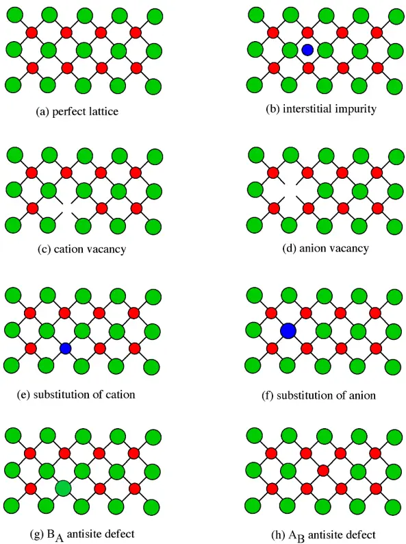
以 A3B5O12石榴石结构为例子,反位缺陷即结构中A格位和B格位离子在晶格热力学不稳定状态下的互相取代。对反位缺陷的研究追溯至 21 世纪初, 捷克科学院物理研究所的研究团队在对 YAG:Ce 和 LuAG:Ce 闪烁单晶的研究中,发现 YAG:Ce 和 LuAG:Ce 的稳态闪烁效率均是 BGO 单 晶的 7~8 倍,它们在 1 μs 门宽时间测得的光产额却分别为 BGO 的 300%和 150%。并探测到大 量慢衰减,与前面的现象相应证。进一步研究得出, 该慢衰减分量是由于能带中浅能级陷阱对自由电子 的俘获,致使 Ce 离子发光中心处复合发光过程受 到延迟。通过低温热释光的方法, YAG:Ce 与 LuAG:Ce 中的浅电子陷阱均得到证实,其中浅电子 陷阱的深度分别为 0.18 eV 和 0.29 eV,在其报 道中指出该类电子陷阱与反位缺陷关系密切。该类 反位缺陷能够与发光中心形成激烈竞争,阻碍载流 子在发光中心处复合,对石榴石闪烁体的光产额和 时间特性有很大的影响。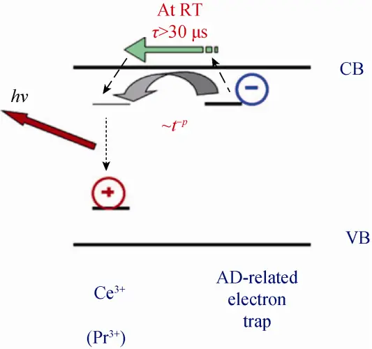
以 LuAG 晶体为例(如图所示),反位缺陷对其造成的影响主要有: 1) 在 300~350 nm 处引起 1 个附加的紫外发射带,形成一个除发光中心(Ce3+, Pr3+)外的又一个载流子弛豫通道; 2) 在禁带中形成 不同深度的附加陷阱能级,该陷阱能级能够俘获输 运过程中的载流子,造成发光延迟。因此,反位缺陷的消除或抑制一直是近些年石榴石闪烁体重要研究内容。为了更好地解决反位 缺陷所带来的问题,研究人员对此展开探究,并提出有效的优化途径:降低制备温度(单晶薄膜与陶瓷)、调节能带结构。参考《石榴石闪烁材料的研究进展-硅酸盐学报》
悬空键(dangling bond)
对于材料最表面的一层原子来说,其外侧没有原子与其键合,配位数少,就产生悬空的化学键,其存在导致表面几层原子偏离正常位置,造成点阵畸变,使其能量高于晶体内部。表面原子层,能量高,不稳定,往往具有较强的化学和催化活性。详细参考这里。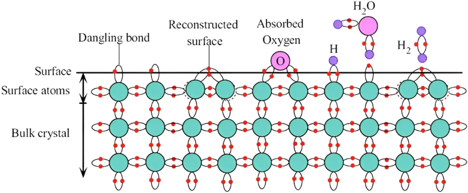
比如对钙钛矿太阳能电池来说,必须尽可能消除钙钛矿材料中的缺陷,而其表面的悬空键会形成缺陷能级,降低电池的光电转换效率,因此人们通过表面钝化的方式消除悬空键的影响。(参考Jiang, Qi, et al. "Surface passivation of perovskite film for efficient solar cells." Nature Photonics 13.7 (2019): 460-466.)
Disordered Structures
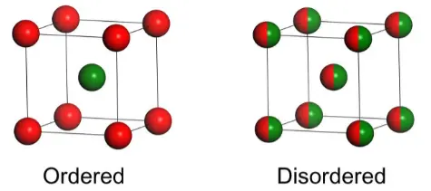
However, for one family of inorganic crystals with disordered structures, such as molybdates and tungstates in which two or more cations statistically occupy the same lattice site, the symmetry of spectroscopic sites for the dopant Ln3+ ions was observed to deviate from that of crystallographic sites. Because the microscopic model of such structural disorder is established from a least-squares fitting of single-crystal X-ray diffraction (XRD) data by standard crystallography analysis, which takes into account those cations randomly occupying the same lattice site as a virtual “average” ion with their respective probabilities, the actual local symmetry of the dopant in the disorder site can not be revealed from the crystallographic data. [Breakdown of Crystallographic Site Symmetry in Lanthanide-Doped NaYF4 Crystals-Angew-2012]
Small polarons
Small polarons: Small polarons are obtained when an excess charge (electron or hole), typically consecutive to the formation of a point defect (donor or acceptor), in a polarizable insulating lattice localize on one single atom instead of being delocalized throughout the crystal. Such localization is concomitant with a polarization distortion of the surrounding matrix (called “self-trapping” distortion) that contributes to create on the site in question a deep electrostatic potential favorable to the localization of the charge [Figs. (c) and (d)]. This electrostatic energy counterbalances the cost associated with the quantum confinement of the charge. The localized charge and its self-trapping distortion cannot be dissociated from each other. Both of them form the entity commonly called as “small polaron.” [mathjax]
Small polarons in SnO2 (perovskite)
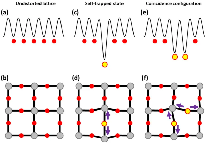
上图是 Schematic representation of a small polaron in a crystal.
- Upper panels: schematic view of the potential felt by the excess charge;
- Lower panels: application to the oxygen-type hole polaron in a perovskite oxide (only one plane of the SnO2 sublattice is shown).
- (a)(b): Undistorted lattice, all the O sites (red circles) are equivalent, the hole is delocalized.
- (c)(d): Self-trapped configuration: the hole polaron is localized on the yellow O atom. It repels the two nearestneighbor Sn atoms (purple arrows), which contribute to stabilize its site.
- (e)(f): Coincidence configuration for hopping: the hole has the same energy whether it is placed on a yellow O or on the other.
Migration of Small Polarons
The migration of small polarons is a thermally activated phenomenon. However, such thermal activation does not result from the thermal overbarrier motion of the electronic charge itself. The motion of the charge is indeed, intrinsically, a tunneling process. But, such tunneling is not likely to take place in the stable, self-trapped, configuration because the charge is strongly trapped in the potential well caused by the surrounding self-trapping distortion, making the neighboring sites of high energy with respect to the self-trapped site [Figs. (c) and (d)]. For such tunneling to occur, it is necessary that the crystal around be distorted until one neighboring site has the same energy as the polaron site, producing degenerate (diabatic) energy levels, a state called “coincidence configuration” [Figs. (e) and (f)]. Such distortion can be produced by the thermal agitation of the surrounding atoms, with a probability \(\propto e^{-E_{c} / k_{_B} T}\) , where \( E_c\) is the coincidence energy, i.e., the energy of the most stable coincidence configuration with respect to the stable self-trapped one. The coincidence energy Ec plays the role of an activation energy for the hopping process of the polaron. The hopping rate for the small polaron hopping is thus \(\propto e^{-E_{c} / k_{_B} T}\) , but the energy in this Arrhenius term, to be paid by thermal agitation, is related to the motions of the surrounding atoms, not to the motion of the electronic charge itself. According to the typical tunneling probability in the coincidence configuration, compared to the time scale of the coincidence, the transfer can be adiabatic (i.e., the electronic charge has the time to tunnel), nonadiabatic (i.e., the electronic charge has not the time to tunnel, so that many occurrences of the coincidence are necessary before a jump occurs), or lie in-between. In an adiabatic hopping, the charge is progressively transferred from the initial to the final site, together with the self-trapping distortion.
参考资料:
(1) "DFT+ U study of self-trapping, trapping, and mobility of oxygen-type hole polarons in barium stannate." Physical Review B 96.13 (2017): 134123.
(2) Triplet energy transfer in conjugated polymers. II. A polaron theory description addressing the influence of disorder
(3) Small polaron-Physics Today 35, 6, 34 (1982)
(4) Polarons in crystalline and non-crystalline materials-Advances in Physics-1969
(5) Conduction in glasses containing transition metal ions-Journal of Non-Crystalline Solids-1968
(6) Natanzon Y, Azulay A, Amouyal Y. Evaluation of Polaron Transport in Solids from First‐principles-Israel Journal of Chemistry-2020阅读
(7) Trapping, self-trapping and the polaron family-Journal of Physics: Condensed Matter-2007
缺陷调控实例
YBCO超导体
High temperature superconductors like YBa2Cu3O7-x, have electrical properties controlled by oxygen stoichiometry.
YBa2Cu3O6 = antiferromagnetic insulator
YBa2Cu3O7-x = metallic conductor highest Tc(95 K) x = 0.07
Single crystal film have much higher critical currents than bulk single crystals.
固溶体
参考资料:
(1) Solid Solutions-Teaching & Learning Packages-剑桥大学
(2) aalto
材料中的热力学
MIT
Defects
Why do crystals have defects? 参考
- Up to a certain limit, the presence of defects leads to a reduction of free energy
- Creating a single defect in a perfect crystal:
– Requires a certain amount of energy, ΔH
– Causes a considerable increase in entropy, ΔS, because of the large number of positions which this defect can occupy (configurational entropy) - At some point, there are already so many defects that the energy required to
create more defects will be larger than any subsequent gain in entropy.
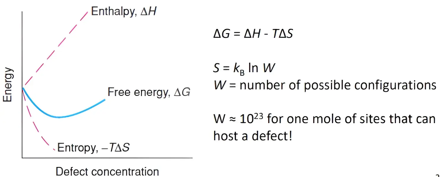
- For a given crystal, a free energy curve can be drawn for every possible type of defect
– The main difference between the curves is the position of the free energy minimum - The dominant defect is the one that is the easiest to form
– Has the smallest ΔH and the free energy minimum occurs at the highest defect concentration
固相反应
Hume-Rothery rules
材料的制备
晶体生长工艺
Micro-pulling-down