Carrier Transport Phenomena
transport processes include:
(1) drift
(2) diffusion
(3) recombination
(4) generation
(5) thermionic emission
(6) space charge effect
(7) tunneling
(8) impact ionization
Carrier Drift
Carrier Drift-mobility
Under thermal equilibrium, the average thermal energy of a conduction electron is \(\displaystyle\frac{1}{2} m_{n} v_{t h}^{2}=\frac{3}{2} k T \), which involvs effective mass of electrons and avergae thermal velocity(at RT, is about \( 10^{7} \mathrm{~cm} / \mathrm{s}\) for Si and GaAs).
Mean free path, typical one \(10^{-5} \mathrm{~cm} \), along with mean free time 1 ps.
Under electrical field, the final motion consists of random thermal motion and drift velocity(due to electrical field). Drift velocity can be written as( at low field) :$$v_{n} = -\mu_{n} E$$ where electron mobilty \( \mu_{\mathrm{n}} \equiv \displaystyle\frac{q \tau_{c}}{m_{n}} \), which describe how strongly the motion of an electron is influenced by an applied electic field.
There is also a counterpart for holes in the valence band: $$v_{p} = \mu_{p}E$$
Regarding mobilty, is propotional to mean free time between two collisions, which in turn is determined by the various scattering mechanisms. Lattice scattering and impurity scattering are the major influence.
(1) Lattice scattering results from thermal vibration of the lattice atoms(disturbed periodic potential field), and the mobility due to lattice scattering is propotional to \( T^{-3 / 2} \).
(2) Impurity scattering happens when a charge carriers travels past an ionized dopant impurity. Travel path will be deflected because of Coulomb force interaction. Obviously, higher concentration of ionized impurities(charged ions), stronger impurity scattering. At higher temperatures, chare carrier move faster in front of the ionized impurities, which makes the interaction time of impurity scattering shorter. In short, mobility due to impurity scattering is \( \mu_{I}=T^{3 / 2} / N_{T}\), where \(N_{T} \) is the total impurity concentration.
Within a unit time, \( \tau_{c}\) times collision would happen due to the various scattering mechanisms. $$\frac{1}{\tau_{c}} = \frac{1}{\tau_{c, \text { lattice }}}+\frac{1}{\tau_{c, \text { impurity }}}$$ or $$\frac{1}{\mu} =\frac{1}{\mu_{L}}+\frac{1}{\mu_{I}}$$
Carrier Drift-Resistivity
When a positive bias in voltage is applied to the right-hand terminal, each electron will experience a force, which is equal to the negative gradient of potential energy, $$-q E=-(\text { gradient of electron potential energy })=-\frac{d E_{C}}{d x}$$Here, the bottom of the CB \(E_{C} \) corresponds to the potential energy of an electron. We can also use other subscript to express parallel cases. For p-n junctions, we often use intrinsic Fermi level \( E_{i} \).
We can define a related quantity \(\psi \) as the electrostatic potential. $$E \equiv-\frac{d \psi}{d x}$$Note that \( \psi \) is electrostatic potential, \( E_{C}\) or \(E_{i}\) is potential energy, \(E\) is electric field.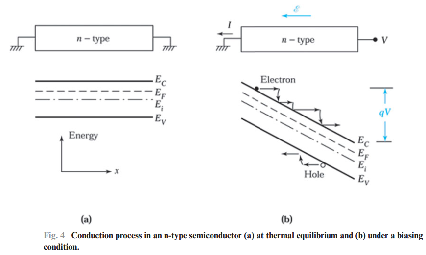
\( \psi=-\displaystyle\frac{E_{i}}{q} \) provides a relationship between the electrostatic potential and the potential energy of an electron.
It should be mentioned that only for homogenous semiconductors as shown above, potential energy decreases linearly with distance. In other words, the electric field is a constant.
The electron current density is $$J_{n}= \frac{I_{n}}{A} =\sum_{i=1}^{n}\left(-q v_{i}\right) =-q n v_{n} = q n \mu_{n} E$$
The total current flowing in the semiconductor due to the additional electric field is $$J = J_{n}+J_{p} =\left(q n \mu_{n}+q p \mu_{p}\right) E$$
The quantity in parentheses is known as conductivity \( \sigma = q\left(n \mu_{n}+p \mu_{p}\right)\). The corresponding resistivity is the reciprocal of \( \sigma\) $$\rho \equiv \frac{1}{\sigma}= \frac{1}{q\left(n \mu_{n}+p \mu_{p}\right)}$$
Generally, in extrinsic semiconductors, we just take only one kind of carriers into consideration due to the large orders-of-magnitude difference between the two carriers densities.
four-point probe method for measuring resistivity
(one small constant current source + one voltmeter)
The resistivity is given by \( \rho = \frac{V}{I} \cdot W \cdot C F\) , where CF is a well-documented “correction factor”(\(C F =4.54 \quad \text { when } d \gg s\)).
It is difficult to measure the impurity concentration, while it is rather easy to measure the resistivity. Therefore, people often use the measured resistivity value to locate the impurity concentration(if complete ionization) according to the well-documented files.
拓展:
(1) 范德堡方法+保角映射
(2) 不同拓扑结构下半导体电阻率特性研究
The Hall Effect
Actually, the concentration of impurities is not exactly the carrier concentration, because only the ionized impurities can serve as carriers. The ratio of the ionized impurities to the total impurities depends on the temperature and impurity energy level. Hall measurement is a frequently-used method to measure the carrier concentration (not impurity concentration), which can also be used to convince people of the existence of holes as charge carriers.
Hall coefficient for n-type: \( R_{H} \equiv \displaystyle\frac{1}{q p}\)
Hall coefficient for p-type: \(R_{H} \equiv - \displaystyle\frac{1}{q n}\)
Carrier Diffusion
Diffusion Process
Diffusion process originates from the spatial varaition of carrier concentration. When it comes to the diffusion process for the carriers in semiconductor materials, we called it "diffusion current". Diffusion current results from the random thermal motion of carriers in a concentration gradient, and is proportional to the spatial derivative of the electron density. Diffusion coefficient(\( D_{n}=v_{t h} l\), thermal velocity times mean free path) is the proportionality factor in Fick's law.$$J_{n} = q D_{n} \frac{d n}{d x}$$
Einstein Relation
For one-dimensional case, by using the theorem for the equipartition of energy, we have \( \displaystyle\frac{1}{2} m_{n} v_{t h}^{2} = \frac{1}{2} k T \)(one degree of freedom),then by simple substitution, we can get the relationship between diffusion coefficient and mobility$$D_{n}=\left(\frac{k T}{q}\right) \mu_{n}$$that characterize carrier transport by diffusion and by drift in a semiconductor.
Current Density Equations
When an electric field is present in addition to a concentration gradient, the electron/hole current densities as well as the total density are as follows:$$\begin{array}{l} J_{n}=q \mu_{n} n E+q D_{n} \displaystyle\frac{d n}{d x} \\ J_{p}=q \mu_{p} p E-q D_{p} \displaystyle\frac{d p}{d x} \\ J_{\text {cond }}=J_{n}+J_{p}\end{array}$$
Generation and recombination processes
- In thermal equilibrium, \( p n=n_{i}^{2}\) is valid.
- Carrier injection—introducing excess carriers, then a nonequilibrium situation, \( p n>n_{i}^{2}\).
- Carrier injection can be realized by optical excitation/forward-biasing a p–n junction
- A nonequilibrium situation is restored to the equilibrium state by recombination of the injected minority carriers with the majority carriers, which can be a photon emission(radiative recombination)/heat dissipation to the lattice(non-radiative recombination).
- Direct recombination (band-to-band recombination), usually dominates in direct-bandgap semiconductors(like GaAs).
- Indirect recombination (via bandgap recombination centers) dominates in indirect-bandgap semiconductors (like Si).
Direct Recombination
Under thermal equilibrium conditions, electron-hole pair generation rate is equal to recombination rate \( G_{t h}=R_{t h} \) so that \( p n=n_{i}^{2} \) is maintained. More specifically, the law of mass action tell us that at equilibrium, the product of the electron concentration and the hole concentration is equal to the square of the intrinsic carrier concentration(\( n_{i}^{2}\)).
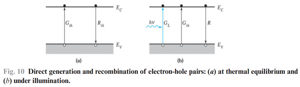 For direct-bandgap semiconductors, direct recombination is efficient, and its rate is proportional to the number of electrons available in CB and the numbers of holes in VB. $$R = \beta n p$$ For n-type semiconductor without any stimulation, if it is in equilibrium state, then it holds true $$G_{t h} = R_{t h} = \beta n_{n o} p_{n o}$$When we shine a light on the semiconductor to produce electron-hole pairs at a rate \( G_{L}\), the recombination and generation rate become(subscript n means n-type, o means equilibrum, \(\Delta n \) and \( \Delta p \) represent the excess carriers due to external stimulation(carrier injection))$$\begin{array}{c} R=\beta n_{n} p_{n}=\beta\left(n_{n o}+\Delta n\right)\left(p_{n o}+\Delta p\right) \\ G=G_{L}+G_{\mathrm{th}} \end{array}$$where excess carrier concentrations $$\begin{array}{l} \Delta n=n_{n}-n_{n o} \\ \Delta p=p_{n}-p_{n o} \\ \Delta n =\Delta p \end{array}$$The net rate of change of hole concentration is given by $$\frac{d p_{n}}{d t}=G-R=G_{L}+G_{t h}-R$$In steady state, we have \( G_{L}=R-G_{t h} \equiv U \), where \( U\) is the net recombination rate, more specifically, the change rate of excess carrier concentration. Note that \( G_{L}=R-G_{t h}\) holds true only for steady state(not mean equilibrium due to the excitation), while \(R-G_{t h} \equiv U \) is true in any cases, specially, for thermal equilibrium or nonequilibrium but steady state, \(U=0\). Here, we are focusing on \(U\) during the transition period from nonequilibrium but staedy state to thermal equilibrium state. Simple substitutions yield(remember \(\Delta n=\Delta p\))$$U=\beta\left(n_{n o}+p_{n o}+\Delta p\right) \Delta p$$Considering \( p_{n o}<<n_{n o}\) and low-injection(small \( \Delta p \)), we can rewrite the equation as follows: $$U \cong \beta n_{n o} \Delta p=\frac{p_{n}-p_{n o}}{\frac{1}{\beta n_{n o}}}$$To make it simpler, we have net recombination rate $$U=\frac{p_{n}-p_{n o}}{\tau_{p}}$$where the excess minority carriers lifetime \( \tau_{p} \equiv \displaystyle\frac{1}{\beta n_{n o}}\). The physical meaning of lifetime can best be illustrated by the transient response of a device after the sudden removal of the light source.
In a word, after the removal of of light, the net recombination rate is from the excess minority carriers in CB and the "equilibrium state majority carrier" in VB for n-type semiconductors, i.e. \( U \cong \beta n_{n o} \Delta p \).
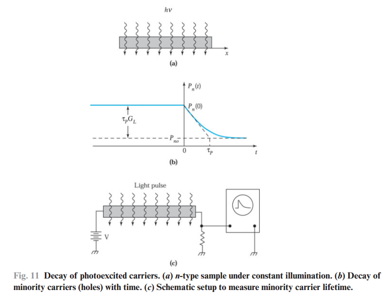
(1) When light is on, it's not in thermal equilibrium any more. Then after a "charging time", it reaches steady state(nonequilibrium).
(2) If at \( t=0 \), the light is suddenly turned off. The boundary condition \( p_{n}(t=0)=p_{n o}+\tau_{p} G_{L} \) and \(p_{n}(t \rightarrow \infty)=p_{n 0} \).
(3) According to \( \displaystyle\frac{d p_{n}}{d t}=G_{\mathrm{th}}-R=-U=-\frac{p_{n}-p_{n 0}}{\tau_{p}}\), we obtain the solution:$$p_{n}(t)=p_{n o}+\tau_{p} G_{L} \exp \left(-t / \tau_{p}\right)$$Note that \( \tau_{p} G_{L}\)(constant) is what we can measured readily as shown in the following figure.
Measure of the lifetime of the excess minority carriers
(1) The increase in conductivity manifests itself by a drop in voltage across the sample when a constant current is passed through it.
(2) The double sided arrow represent excess carrier concentration at equilibrium state due to light.
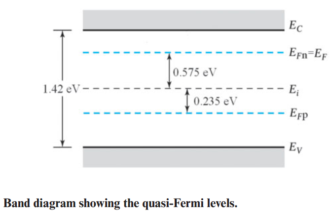
Quasi-Fermi Level
- The Fermi-level \( E_{F}\) is meaningful only in the thermal equilibrium state without any excess carriers(no extra stimulation, if not, then \( p n>n_{i}^{2} \)).
- The quasi-Fermi levels \(E_{F n} \) and \(E_{F p} \) are used to express the electron and hole concentrations in nonequilibrium state and are defined by the following equations:$$\begin{array}{l} n = n_{i} e^{\left(E_{F n} -E_{i}\right) / k T} \\ p = n_{i} e^{(E_{i}-E_{F p})/ k T} \end{array}$$
- The separation of the quasi-Fermi levels is a direct measure of the deviation from equilibrium. It is very useful to visualize majority and minority carrier concentrations varying with position in devices.
Indirect Recombination
A direct transition that conserves both energy and momentum is not possible without a simultaneous lattice interaction. Therefore the dominant recombination process in such semiconductors is indirect transition via localized energy states in the forbidden energy gap.
These localized energy states(intermediate-level states) are also called recombination centers. By assuming equal electron and hole capture cross sections, that is, \(\sigma_{n}=\sigma_{p}=\sigma_{o} \), we can get simplified expression of recombination rate: $$U=v_{t h} \sigma_{o} N_{t} \frac{\left(p_{n} n_{n}-n_{i}^{2}\right)}{p_{n}+n_{n}+2 n_{i} \cosh \left(\frac{E_{t}-E_{i}}{k T}\right)}$$ Under a low-injection condition in an n-type semiconductor \( n_{n} \gg>p_{n}\), the recombination rate can be written as $$U \approx v_{t h} \sigma_{o} N_{t} \frac{p_{n}-p_{n o}}{1+\left(\frac{2 n_{i}}{n_{n o}}\right) \cosh \left(\frac{E_{t}-E_{i}}{k T}\right)}=\frac{p_{n}-p_{n o}}{\tau_{p}}$$ which is similar to the case of direct recombination, however, \( \tau_{p} \) depends on the locations of the recombination centers in the bandgap.
Surface Recombination
Abrupt discontinuity of tha lattice structure at the surface leads to a large number of localized energy states (or generation-recombination centers), which can also be called surface states, may greatly enhance the recombination rate at the surface region. Under some unditions/approximations, the total number of carriers recombining at the surface per unit area and unit time can be simplified to$$U_{s} \cong v_{t h} \sigma_{p} N_{s t}\left(p_{s}-p_{n o}\right)$$
Continuity equation
The governing equation that take all effects (drift, diffusion, recombination, generation) into consideration is called the continuity equation.
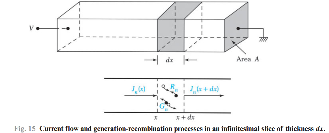
If we are focusing on infinitesimal slice with thickness \( dx \) located at \( x\). The overall rate of change in the number of electrons in the slice is then$$\frac{\partial n}{\partial t} A d x=\left[\frac{J_{n}(x) A}{-q}-\frac{J_{n}(x+d x) A}{-q}\right]+\left(G_{n}-R_{n}\right) A d x$$By taylor expansion, we get: $$J_{n}(x+d x) = J_{n}(x)+\frac{\partial J_{n}}{\partial x} d x+\ldots$$We thus obtain the basic continuity equation for electrons: $$\frac{\partial n}{\partial t}=\frac{1}{q} \frac{\partial J_{n}}{\partial x}+\left(G_{n}-R_{n}\right)$$A similar continuity can be derived for holes (watch out for the minus sign)$$\frac{\partial p}{\partial t}=-\frac{1}{q} \frac{\partial J_{p}}{\partial x}+\left(G_{p}-R_{p}\right)$$
Compare the above equations with \(\nabla \cdot \vec{j}+\frac{\partial \rho}{\partial t}=0 \) in electrodynamics lesson.
For the one-dimensional case under low-injection condition, the continuity equations for minority carriers(use expressions to replace \(J_{n} \), \(J_{p} \), \( R_{n} \), \(R_{p} \))$$\begin{array}{c} \displaystyle\frac{\partial n_{\mathrm{p}}}{\partial t}=n_{\mathrm{p}} \mu_{\mathrm{n}} \frac{\partial E}{\partial x}+\mu_{\mathrm{n}} E \frac{\partial n_{\mathrm{p}}}{\partial x}+D_{\mathrm{n}} \frac{\partial^{2} n_{\mathrm{p}}}{\partial x^{2}}+G_{\mathrm{n}}-\frac{n_{\mathrm{p}}-n_{\mathrm{p} 0}}{\tau_{\mathrm{n}}} \\ \displaystyle\frac{\partial p_{\mathrm{n}}}{\partial t}=-p_{\mathrm{n}} \mu_{\mathrm{p}} \frac{\partial E}{\partial x}-\mu_{\mathrm{p}} E \frac{\partial p_{\mathrm{n}}}{\partial x}+D_{\mathrm{p}} \frac{\partial^{2} p_{\mathrm{n}}}{\partial x^{2}}+G_{\mathrm{p}}-\frac{p_{\mathrm{n}}-p_{\mathrm{n} 0}}{\tau_{\mathrm{p}}} \end{array}$$
It is rather easy to remember the equation. The left side is the change of minority carriers in terms of time, and the right side is made up of three parts:
(1) the influence of the electric filed gradient and the minority carrier gradient (similar with "flow conservation")
(2) Fick's second law like \( \displaystyle\frac{\partial \varphi}{\partial t}=D \frac{\partial^{2} \varphi}{\partial x^{2}}\)
(3) minority carriers generation rate
(4) net recombination rate
In addition to the continuity equations, Poisson’s equation(\(\nabla^{2}\Phi=-{\rho}/\epsilon_{0}\), a minus sign) $$\frac{\mathrm{d} E}{\mathrm{~d} x}=\frac{\rho_{\mathrm{s}}}{\varepsilon_{s}}=\frac { q\left(p-n+N_{D}^{+}-N_{A}^{-}\right)}{\varepsilon_{s}}$$must be satisfied, where \( \rho_{\mathrm{s}} \) is the semiconductor dielectric permittivity and \( \rho_{s}\) is is the space charge density given by the algebraic sum of the charge carrier densities and the ionized impurity concentrations \( q\left(p-n+N_{D}^{+}-N_{A}^{-}\right) \). What's more, the the space charge density here is one-dimensional, which means the dimension of \(\rho_{s}dx \) is "1". Note that, the above equation is the same as the Gauss's law in the differential form with respect to one/two/three dimension \(\nabla \cdot \mathbf{E}=\rho / \epsilon_{0}\).
Note that when we say space charge density, we are talking about postive charges.
Steady-State Injection from One Side
The following figure shows the n-type semiconductor in which excess carriers are injected from one side as a result of illumination. It is assumed that light penetration is negligibly small(i.e., the assumptions of zero electric field \(E =0\) and zero generation \(G =0\) for \( x>0 \)). At steday state, there is a concentration gradient near the surface.
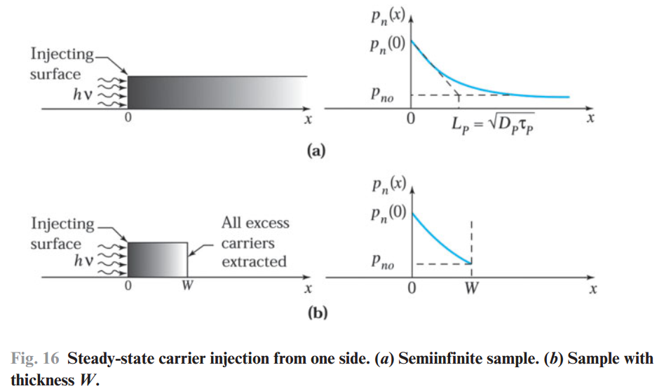 The differential equation for minority carriers inside the semiconductor is $$\frac{\partial p_{n}}{\partial t}=0=D_{p} \frac{\partial^{2} p_{n}}{\partial x^{2}}-\frac{p_{n}-p_{n o}}{\tau_{p}}$$Boundary conditions:
(1) \(p_{n}(x=0)=p_{n}(0)=\text { constant value } \)
(2) \(p_{n}(x \rightarrow \infty)=p_{n o}\)
Solution: $$p_{\mathrm{n}}(x)=p_{\mathrm{n} 0}+\left[p_{\mathrm{n}}(0)-p_{\mathrm{n} 0}\right] \exp \left(-\frac{x}{L_{\mathrm{p}}}\right)$$where diffusion length \( L_{p}= \sqrt{D_{p} \tau_{p}} \).
For the case in figure(b), we have the condition that at \( x=W \), \( p_{\mathrm{n}}(W)=p_{\mathrm{n} 0} \). The final solution becomes:$$p_{\mathrm{n}}(x)=p_{\mathrm{n} 0}+\left[p_{\mathrm{n}}(0)-p_{\mathrm{n} 0}\right] \frac{\sinh \left(\frac{W-x}{L_{\mathrm{p}}}\right)}{\sinh \left(\frac{W}{L_{\mathrm{p}}}\right)}$$
Differential equation solving, see my note MIT-微分方程-1
Minority Carriers at the Surface
The Haynes-Shockley Experiment
Thermionic emission process
If carriers have sufficient energy, they may be "thermionically" emitted into the vacuum. This is called the thermionic emission process. The electron affinity is \( q \chi\), and work function is \( q \phi_{s} \). It is clear that an electron can be thermionically emitted into the vacuum if its energy is above \( q \chi \).
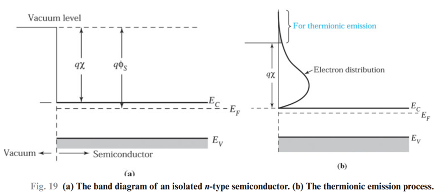 The electron density with energies above \( q \chi\) can be obtained from an expression similar to that for electron density in the conduction band except that the lower limit of the integration is \( q \chi\) instead of \( E_{C} \). $$n_{\mathrm{th}}=\int_{q \chi}^{\infty} n(E) d E=N_{\mathrm{C}} \exp \left[-\frac{q\left(\chi+V_{\mathrm{n}}\right)}{k T}\right]$$where \(N_{C} \) is the effective density of states in the conduction band, and \( V_{n}\) is the difference between the bottom of the conduction band and the Fermi level.
Work function: wikidot 功函数的基本概念 光电效应
Here(solid state physics), the electron affinity is defined differently than in chemistry
Tunneling process

The first figure shows the energy band diagram. The potential barrier height between the two isolated semicoductors \(q V_{0} \) is equal to the electron affinity \(q \chi \). If the distance is small enough, then electrons(even energy less than the barrier height) in the left semiconductor may transport across the barrier and move to the right side. This process is assocaited with the "quantum tunneling phenomenon". The behavior of a particle (e.g. a conduction electron) in the region where \(q V(x)=0 \) can be descirbed by the Schrödinger equation:$$\frac{\hbar^{2}}{2 m_{n}} \frac{d^{2} \psi}{d x^{2}}= E \psi$$The solutions are $$\begin{array}{l} \psi(x) = A e^{j k x}+B e^{-j k x} \quad x \leqq 0 \\ \psi(x) = C e^{j k x} \quad x \geqq d \end{array}$$ where \(k \equiv \sqrt{2 m_{n} E / \hbar^{2}}\).
Inside the potential barrier, the wave equation is given by $$\frac{\hbar^{2}}{2 m_{n}} \frac{d^{2} \psi}{d x^{2}}+q V_{0} \psi = E \psi$$The solution for \(E<q V_{0}\) is $$\psi(x)=F e^{\beta x}+G e^{-\beta x}$$where \( \beta \equiv \sqrt{2 m_{n}\left(q V_{0}-E\right) / \hbar^{2}} \)
According to the continuity requirement and boundary condition, we provides four relations between the five coefficients (\( A\), \( B\), \( C\), \( F\), and \( G\)). We can solve for \( (C / A)^{2}\), which is the transmission coefficient: $$\left(\frac{C}{A}\right)^{2}=\left[1+\frac{\left(q V_{0} \sinh \beta d\right)^{2}}{4 E\left(q V_{0}-E\right)}\right]^{-1}$$When \(\beta d>>1\), the transmission coefficient becomes quite small and varies as$$\left[\frac{C}{A}\right]^{2} \sim \exp (-2 \beta d)=\exp \left[-2 d \sqrt{2 m_{n}\left(q V_{0}-E\right) / \hbar^{2}}\right]$$
Space-charge effect
High-field effect
For carrier drift, we have \(v_{n}=-\mu_{n} E\) for electrons with the electron mobility \(\mu_{\mathrm{n}} \equiv \frac{q \tau_{c}}{m_{n}}\). That the drift velocity is linearly propotional to the applied field is only valid at low electric-fields. We assume that the time interval between collision \(\tau_{c}\) is independent of the applied field. This is a reasonable assumption as long as the drift velocity is small compared with the thermal velocity of carriers, which is about \(10^{7} \mathrm{~cm} / \mathrm{s}\) for Si at RT.
As the velocity approaches the thermal velocity, the dependence of drift velocity on electric filed will begin to depart from the linear relationship. In other words, initially the field dependence of the drift velocity is linear, corresponding to a constant mobility. As the electric field is increased, the drift velocity increases less rapidly. At sufficiently large fields, the drift velocity approaches a saturation velocity. The experimental results can be approximated by the empirical expression $$v_{n}, v_{p}=\frac{U_{s}}{\left[1+\left(\mathscr{E}_{0} / \mathscr{E}\right)^{\gamma}\right]^{1 / \gamma}}$$where \(v_{s}\) is the saturation velocity (\(10^{7} \mathrm{~cm} / \mathrm{s}\) for Si at \(300 K\)), \( \mathscr{E}_{0}\) is a constant. Velocity saturation at high fields is particularly likely for field-effect transistors (FETs) with very short channels.
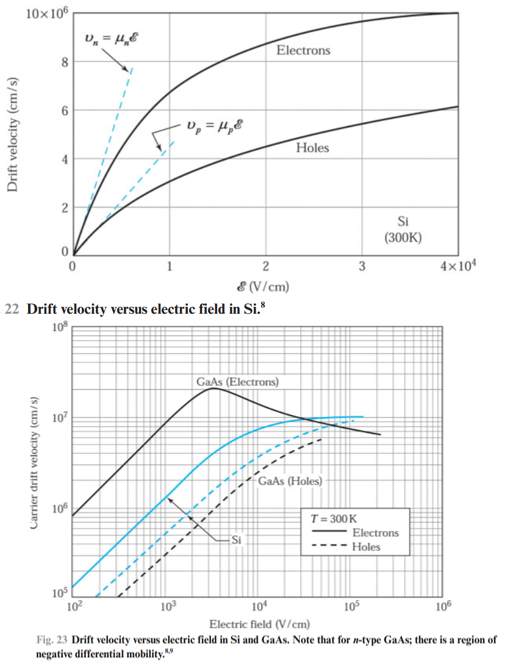
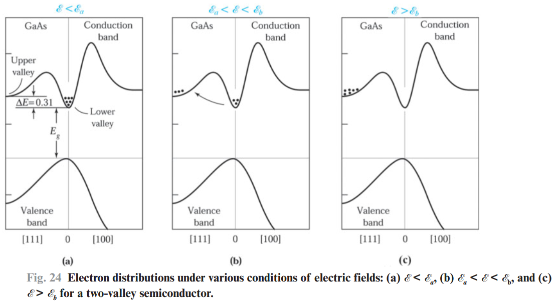
Note that for n-type GaAs, the drift velocity reaches a maximum, then decreases as the field further increases. This phenomenon is due to the energy-band structure of GaAs, which allows the transfer of the conduction electrons from a high-mobility energy minimum (called a valley) to low-mobility, higher-energy satellite valleys, that is, electron transfer from the central valley to the satellite valleys along the [111] direction. This is called the transferred-electron effect.
 When the electric field in a semiconductor is increased above a cetain value, the carriers gain enough kinetic energy to generate electron-hole pairs by the avalanche process. The avalanche process is also referred to as the impact ionization process. This process will result in breakdown in the p–n junction as discussed in other section.

The number of electron-hole pairs generated by an electron per unit distance traveled is called the ionization rate for the electron, \(\alpha_{n}\). Similarly, \(\alpha_{p}\) is the ionization rate for the holes. Both \(\alpha_{n}\) and \(\alpha_{p}\) are strongly dependent on the electric field. The electron-hole pair generation rate \(G_{A}\) from the avalanche process is given by $$G_{A}= \frac{1}{q}\left(\alpha_{n}\left|J_{n}\right|+\alpha_{p}\left|J_{p}\right|\right)$$This expression can be used in the continuity equation for devices operated under an avalanche condition.