激子
激子和Self-Trapped Exciton (STE) Emission
激子:价带中的电子吸收小于禁带宽度的光子能量也能离开价带,但是因为能量不够还不能跃迁到导带成为自由电子。这时,电子实际上还与空穴保持库伦相互作用力,形成一个电中性的系统,称为激子。激子可以作为整体在固体中运动,它可以传播能量和动量,但是不传播电荷(不引起电流)。晶体中,激子产于光吸收、发光、能量传递和光化学等过程。
参考资料:
(1) White-Light Emission from Layered Halide Perovskites-Acc. Chem. Res-2018
(1) 半导体的激子效应及其在光电子器件中的应用-江德生
(2) White-Light Emission from Layered Halide Perovskites-Acc. Chem. Res-2018
(3) 白光LED:如何化繁为简?-Light新媒体
(2) Dynamic Exciton Polaron in Two-Dimensional Lead Halide Perovskites and Implications for Optoelectronic Applications-Acc. Chem. Res-2022
(3) Difference between PL Band Edge Emission and Emission due to Free Exciton
(4) 同步辐射应用基础-邹崇文
(x) Self-Trapped Excitons in All-Inorganic Halide Perovskites: Fundamentals, Status, and Potential Applications-JPCL-2019
激子的吸收:
(1) 在特殊材料中,光子被吸收后会产生激子,从而使这些材料具有更窄的吸收峰,更长的吸收波长等特殊性质。
(2) 实验发现,在带间吸收边的低能一侧,往往会出现一系列分立的吸收峰。谱峰的分布也有一定的规律性。下图是低温下高纯GaAs带边附近的吸收谱。与图中右下角表示的GaAs带间吸收边比较,其主要特征是在吸收边低能一侧出现一系列吸收峰。其吸收强度比带间跃迁吸收强度高得多。图中标号n=1,2,3... ∞∞的吸收谱被归结为自由激子的吸收。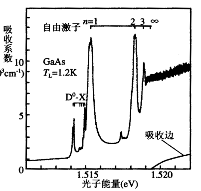 (3) 一般激子吸收和发光的实验都要在低温下进行。碱卤晶体的激子束缚能较高,如LiF的激子束缚能高达 1000meV 。
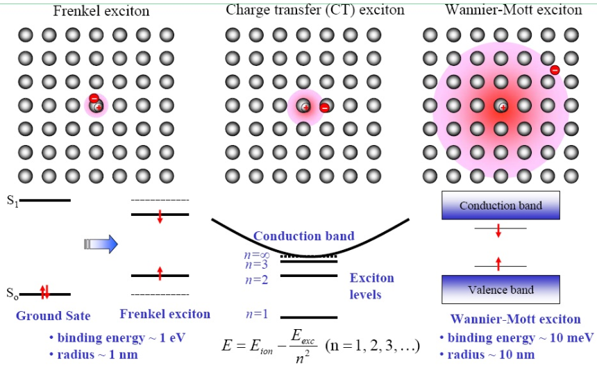
(4) 根据激子结合能的大小,提出两种激子模型。一种称为紧束缚激子或弗仑克尔(Frenkel)激子,它的束缚半径比较小,大约在一个原子的范围内。另一种称为松束缚激子或万尼尔(Wannier-Mott)激子,它的束缚半径比较大,大约为数十个到上百个玻尔半径大小。
(5) 在直接带隙半导体和间接带隙半导体的光吸收边附近存在激子吸收,相应的激子分别称为直接激子和间接激子。(固体发光材料—P86)
激子束缚能也就是激子结合能,是指把库仑力束缚着的激子变为自由的电子和空穴所需要的能量,即从localized变为delocalized。激子能级和氢原子光谱有相似性,离导带越近,能级分布越密,低温下激子的吸收更明显。光学带隙 + 激子结合能 = 电学带隙。
Free netural exiton: 本身的复合发光:能量比band edge emission低
(含有激子发光的详细PDF)。
经典实例

(1) BaS:Eu2+
The appearance of infrared emission is related to the position of the 5d excited level of Eu2+ relative to the conduction band of BaS, which leads to autoionization of the Eu2+ centers upon 4f7-4f65d excitation and the formation of impurity trapped excitons. 参考["Anomalous photoluminescence in BaS: Eu." Physical Review B 74.3 (2006): 035207.]
(2) CaWO4
对于荧光粉来说,基质晶格的吸收的光跃迁可以简单地分为两类:导致自由电荷载流子的光吸收跃迁和不能导致自由电荷载流子的光吸收跃迁。通过光电导实验可以区别这两类跃迁。对CaWO4来说,WO42-吸收紫外辐射,在钨酸根的激发态中的空穴(在氧上)和电子(在钨上)仍然在一起,它们之间的相互作用的能量很大,使类似发生在ZnS中的离域作用不可能存在。这样束缚在一起的电子-空穴对称为激子。当束缚力特别强,就像CaWO4,电子-空穴对就称为弗伦克尔激子。
Intrinsic luminescence of CaWO4 due to the annihilation of self-trapped excitons forming excited [WO4]2− anions give rise to the broad emission spectra peaking around 420 nm.
参考:[固体发光材料—P78]
(3) YVO4:Bi3+
Localized exciton luminescence in YVO4:Bi3+
Anomalous Trapped Exciton and d–f Emission in Sr4Al14O25:Eu2+